
Get A Quick Quote

Email:
sales@ruggedmaster.com
CONTACT INFORMATION
Address: 3th Floor, B2 Building Yinlong Industry Base, Longgang District,ShenZhen,China
At RUGGEDMASTER, we deliver end-to-end OEM and ODM manufacturing solutions designed to support a wide range of electronic product developments, including rugged tablets, rugged phones, rugged handhelds, rugged laptops, and wearable devices. Backed by extensive expertise in electronic assembly and validation processes, our services are supported by experienced engineering teams and state-of-the-art SMT production facilities.
Through long-standing partnerships with globally recognized component suppliers and authorized distributors, we maintain strong advantages in large-volume sourcing while ensuring consistent component quality. Combined with precision SMT mounting and DIP assembly technologies, our advanced manufacturing processes guarantee stable soldering performance, product reliability, and consistent production quality across all delivered solutions.
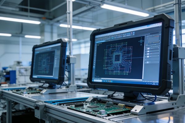
RUGGEDMASTER’s PCB engineering team brings extensive hands-on expertise in circuit board design, focusing on optimizing both product performance and production efficiency. Utilizing industry-standard PCB development platforms such as Allegro, PADS, Protel, ORCAD, Altium Designer (AD), and PADS Logic, our engineers develop layouts precisely aligned with customer-defined functional requirements.
Additionally, we are capable of converting customer-provided PDF schematics into ORCAD-compatible formats and seamlessly generating corresponding netlists, ensuring accurate data integration and efficient transition into subsequent design and manufacturing stages.
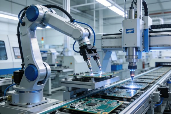
Copper-clad laminate preparation → panel cutting → reference hole punching and positioning drilling → precision CNC drilling → quality inspection → edge deburring → chemical copper deposition → electrolytic copper plating → inspection verification → surface brushing treatment → dry film lamination (or screen printing application) → exposure and development (or thermal curing) → inspection and circuit repair → pattern electroplating (Cu + Sn/Pb) → photoresist stripping → circuit etching → inspection and defect correction → connector area nickel-gold plating → thermal cleaning process → electrical conductivity and continuity testing → surface cleaning → solder mask printing → curing process → legend and marking printing → final curing → surface finishing → cleaning and drying → final quality inspection → protective packaging → completed PCB product.
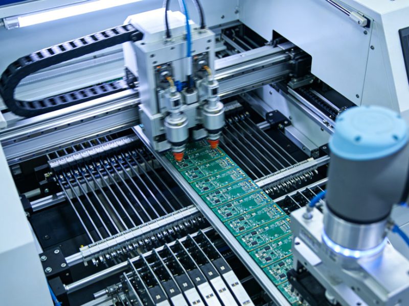
Surface Mount Technology (SMT) represents one of the most widely adopted manufacturing processes in modern electronic assembly. SMT production involves a complete set of precision mounting procedures performed on PCB substrates to achieve high-density and reliable component integration. Our SMT production lines are equipped with advanced manufacturing systems, including Siemens and Panasonic placement machines, Heller reflow soldering equipment, DEK/MPM solder paste printers, as well as KY SPI and VI AOI inspection systems, ensuring consistent assembly accuracy and superior soldering quality.
The standard SMT manufacturing workflow includes: solder paste printing → component placement → thermal curing → reflow soldering → automated optical inspection (AOI) → rework and correction → PCB depaneling → edge finishing → board cleaning.
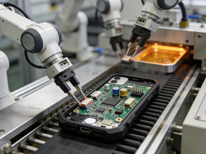
Dual In-line Package (DIP) assembly is an essential stage within the overall PCBA manufacturing process, primarily used for mounting through-hole components that are not suitable for surface mount installation. These components are securely integrated into the circuit board and finalized through wave soldering and subsequent finishing procedures to complete the PCBA assembly. Our dedicated DIP production lines are supported by professionally configured workstations, conveyor systems, and specialized carriers, enabling improved operational efficiency and stable production performance. Strict quality control measures are implemented throughout the process to ensure all assemblies comply with customer-defined quality standards.
The standard DIP assembly workflow includes: component insertion → wave soldering → lead trimming → post-solder finishing → board cleaning → final quality inspection.
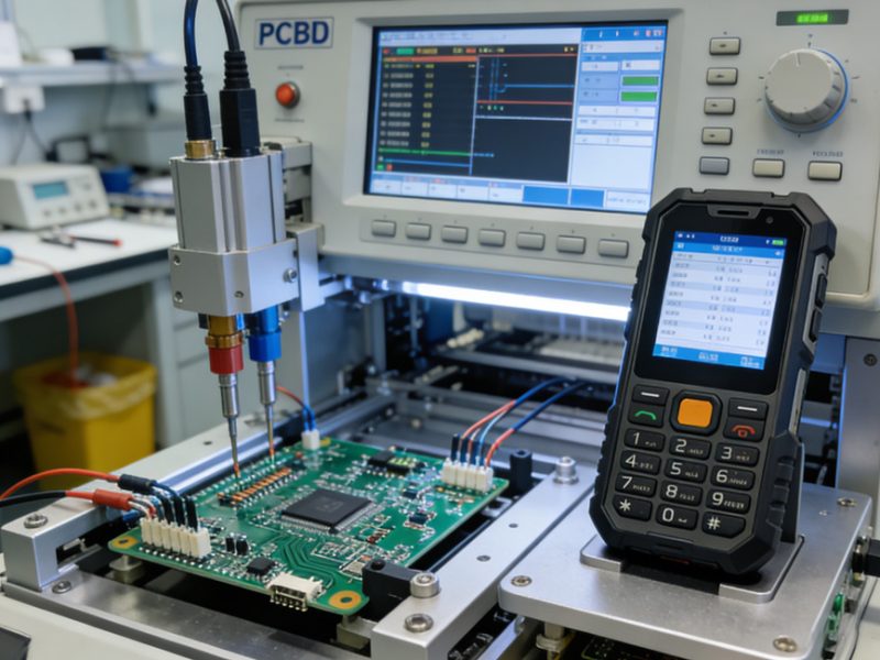
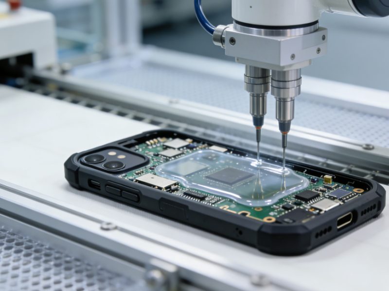
To ensure reliable operation of PCBA assemblies and electronic products in demanding environments, a conformal protective coating is applied to the circuit boards. This protective layer enhances insulation performance while providing resistance against moisture, leakage, vibration, dust, corrosion, aging, and mold formation. It also helps prevent component loosening and improves resistance to electrical corona effects, effectively extending both the storage stability of PCBA modules and the overall service lifespan of electronic devices.

